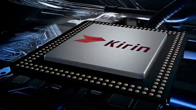
In a bold declaration that could reshape the global semiconductor landscape, Huawei Technologies has announced an ambitious plan to achieve 1.4nm-class chip manufacturing by 2031. This remarkable feat, if realized, would see a substantial 55% increase in transistor density, all while circumventing the critical dependency on advanced EUV (Extreme Ultraviolet) lithography equipment, which is currently inaccessible to the Chinese tech giant due to U.S. trade sanctions.
The core of Huawei's proposed breakthrough lies in its innovative 'LogicFolding' chip design framework. This new architectural approach is designed to dramatically boost transistor density and power efficiency through novel stacking and integration techniques, rather than relying solely on the shrinking features enabled by EUV. Accompanying this, Huawei introduces what it terms the 'Tau Scaling Law,' intended to serve as a successor to Moore's Law, dictating how future chip performance and density will advance.
Affiliate contentGames up to -90% off
Instant key delivery on Instant Gaming
Browse deals →This strategic move by Huawei is a direct challenge to the established norms of semiconductor scaling and a clear attempt to mitigate the impact of ongoing sanctions. By focusing on architectural innovation and alternative scaling methodologies, the company aims to independently push the boundaries of chip technology. This could potentially allow China to narrow the technological gap with industry leaders like TSMC and Nvidia, who heavily rely on EUV for their cutting-edge designs.
The implications of such a breakthrough are vast, offering a potential pathway for China to reduce its reliance on Western technology and establish greater self-sufficiency in the critical semiconductor sector. While met with skepticism by some, Huawei's announcement signals a resolute commitment to innovation despite geopolitical pressures, and sets a new benchmark for competitive long-term technological development.